Skip to content
LasX — The Laser Experts
Contact us

Industry

Diagnostics & Lab-on-a-Chip

LasX builds precision laser systems for diagnostic device manufacturing and runs contract production of microfluidic and biosensor components in an ISO 13485 facility with cleanroom capability.

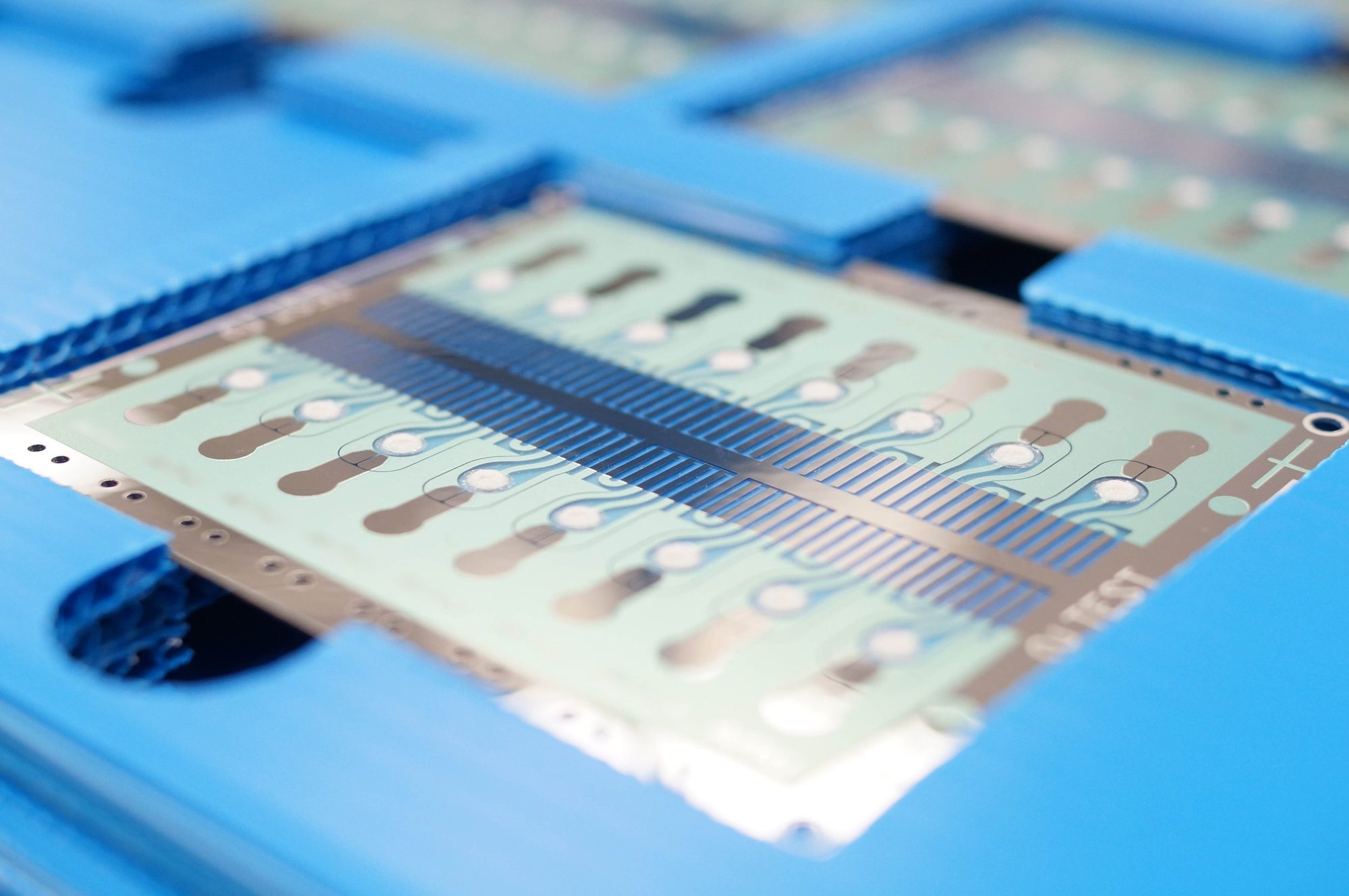
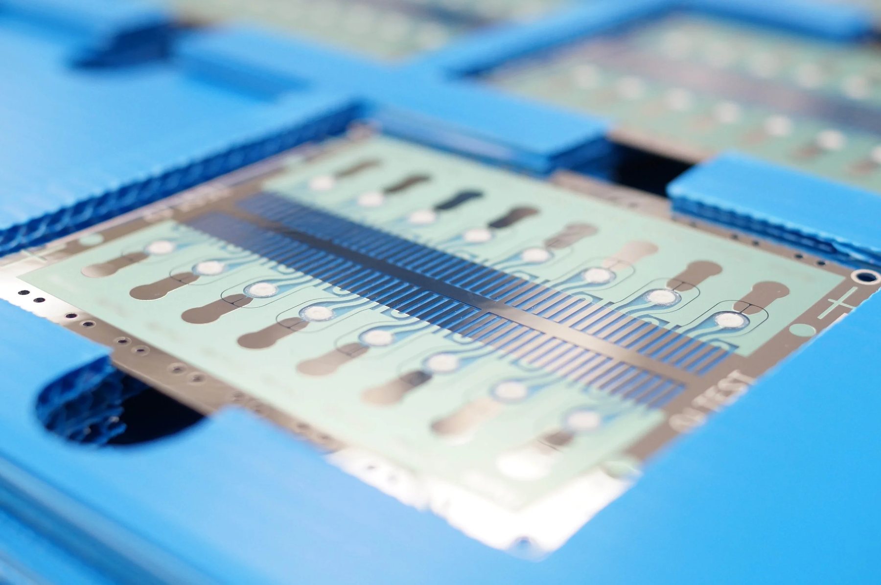
Laser-processed biochip laminate with micro-channel features and electrode pads, in a carrier tray
25 µmDemonstrated feature size
ISO 13485Certified facility
US8016963Precision lamination patent

Applications

What LasX equipment does in Diagnostics & Lab-on-a-Chip

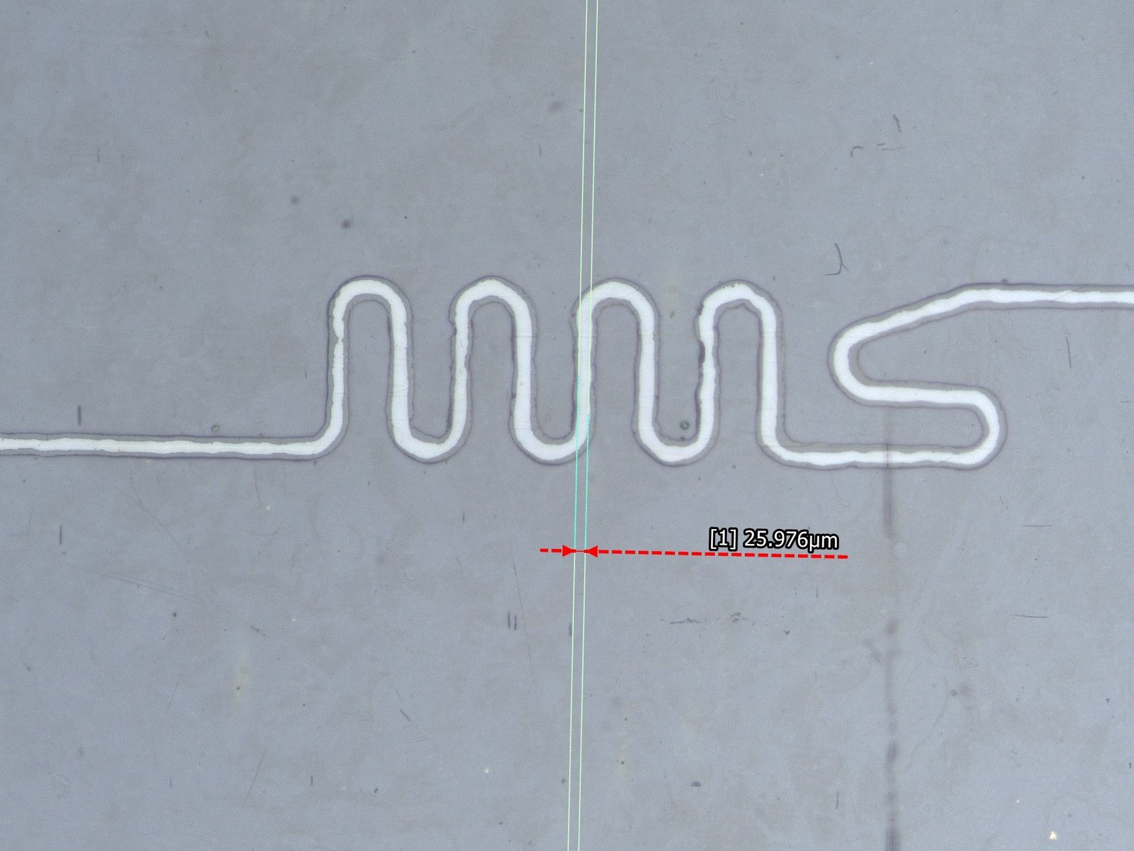
Microscope image of a 26 µm serpentine microfluidic channel laser-cut in double-sided acrylic adhesive tape on a PET backing, with measurement overlay
Micromachining

25 µm microfluidic channel, laser-cut in double-sided PSA

A serpentine channel 26 µm wide, cut through double-sided acrylic adhesive tape on a PET backing with an ultrashort-pulse laser in the PhotonX Innovation Center. No adhesive stringing, no melt at the bends, backing untouched — and fluid runs the full length. Feature sizes a die can't reach, in the layer your cartridge is already built from. Qualified on your stack, in PhotonX, before you commit to a machine.

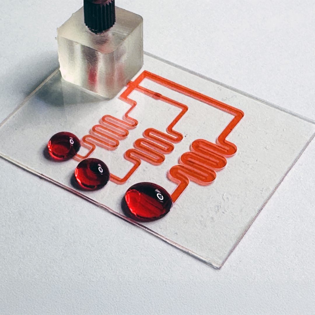
Microfluidic chip with red fluid in serpentine channels
Micromachining

Serpentine mixing channels

Channel geometry comes from the file, so a new mixing path does not need a new tool.

Diagnostic test strips with printed electrodes
Cutting

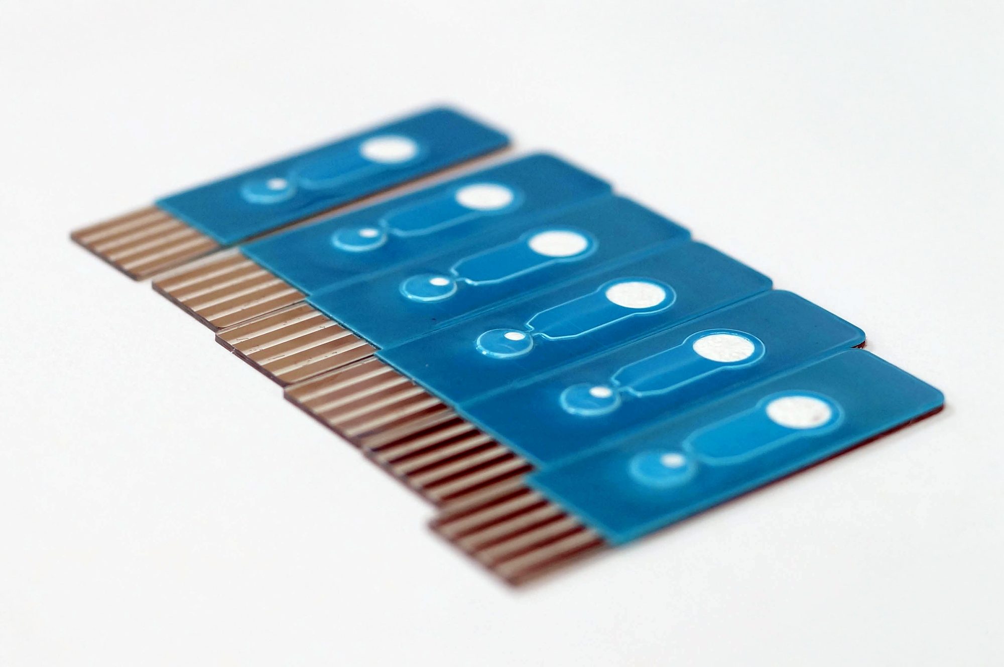
Test strips from electrode laminate

Strips cut from printed electrode laminate, with each sheet registered and compensated for distortion.

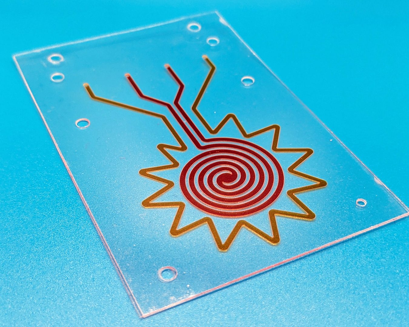
Ablating

Gold biosensor electrodes

Selective ablation of a gold layer patterns custom electrodes. The pattern is a file, so geometry changes without tooling.

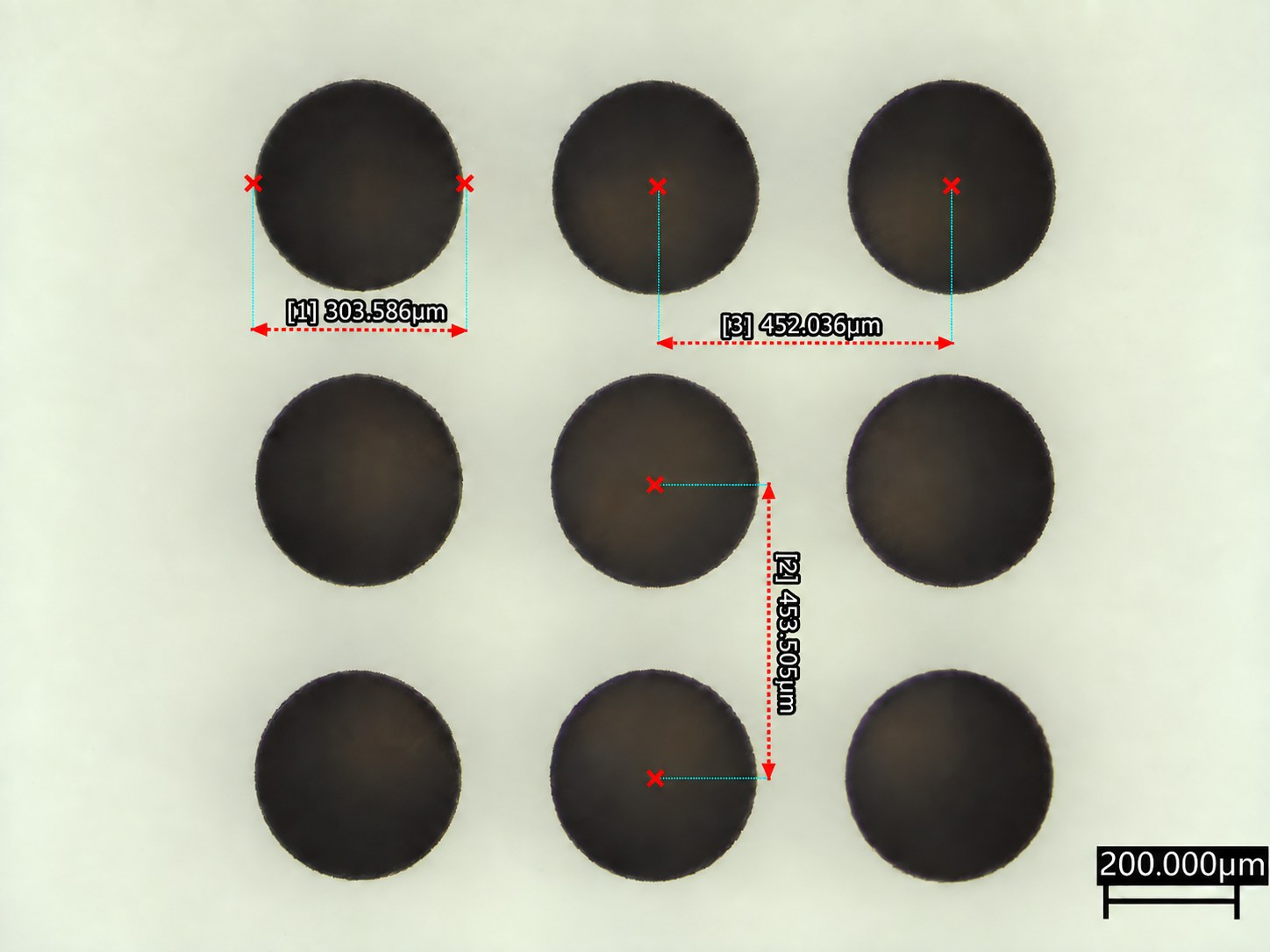
3 × 3 array of 300 µm laser-drilled through-holes in glass on a 450 µm pitch, reflected-light micrograph with measurements
Drilling

Through-holes in glass

Fluid ports and flow-cell vias in glass slides and chips. 300 µm holes on a 450 µm pitch are in development in the PhotonX lab (2026), with diameter and pitch within a few microns of nominal. Taper is the development target.

Why laser, in this market

01

Micron-scale precision for miniaturized devices

Laser micromachining and micro-joining where heat-affected zone and edge condition are measured on the part — across films, laminates, and device components.

02

Consistent processing across multi-material stacks

Stable, validated recipes for polymers, adhesives, thin metals and nitinol, laminates, and glass or silicon — particulate and thermal input controlled to the device requirements you specify.

03

Rapid, tool-less iteration to clean, scalable, compliant manufacturing

CAD-to-part speed and DOE tuning that move from feasibility to a documented process ready for your IQ/OQ/PQ; UDI marks verified to your readability specification, SPC and vision records, and documentation aligned to ISO 13485 and 21 CFR Part 820 — in non-contact, cleanroom-friendly workflows that scale.

Buy the equipment

Buy the equipment

ExactPro registers each sheet of microfluidic laminate and compensates for distortion — mapping the sheet's actual geometry against nominal, which matters most on humidity-sensitive stacks. Positional repeatability is 10 µm, and the cleanroom configuration is standard.

  • Feature size is set by the laser module — features to 25 µm demonstrated in the PhotonX lab with NIR, green, and UV sources
  • XY-stage processing of multi-feature panels, registered sheet by sheet
  • Precision lamination and cutting in one workflow
Have us make the parts

Have us make the parts

Contract production of microfluidic laminates, biosensor electrodes, and cut-and-laminate assemblies, including biosensor electrode modification and fertility-diagnostic devices.

  • Design iterations at file speed during development
  • Validated production without your own capital

A microfluidic device works or fails on geometry a human eye cannot see. At this scale, process control is not a differentiator — it is the product.

More from production

Spiral microfluidic chip with dye in the channels
Spiral channel geometry.
Sheets of diagnostic test strips in blue trays
Strip sheets in production trays.
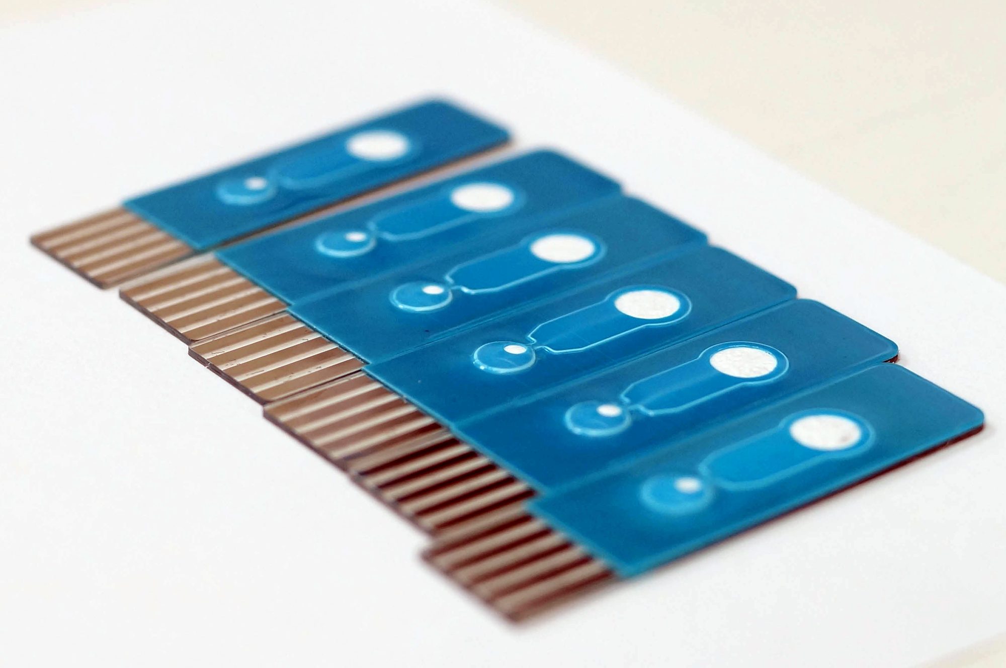
Row of diagnostic test strips
Singulated strips.
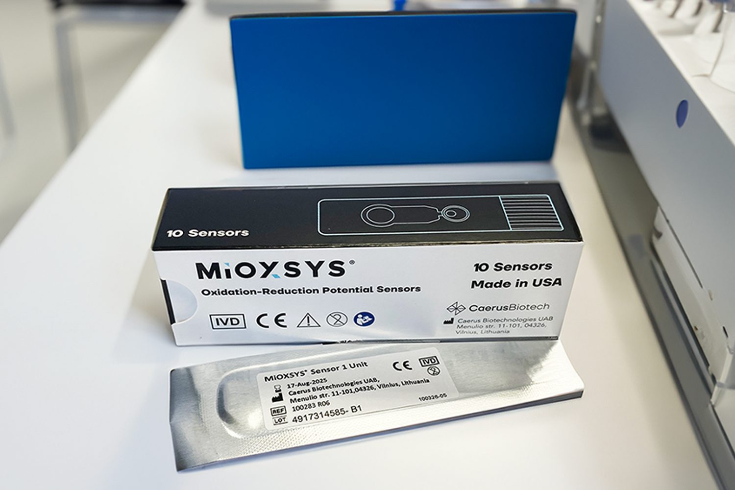
Boxed diagnostic sensors
Finished sensors, packed.
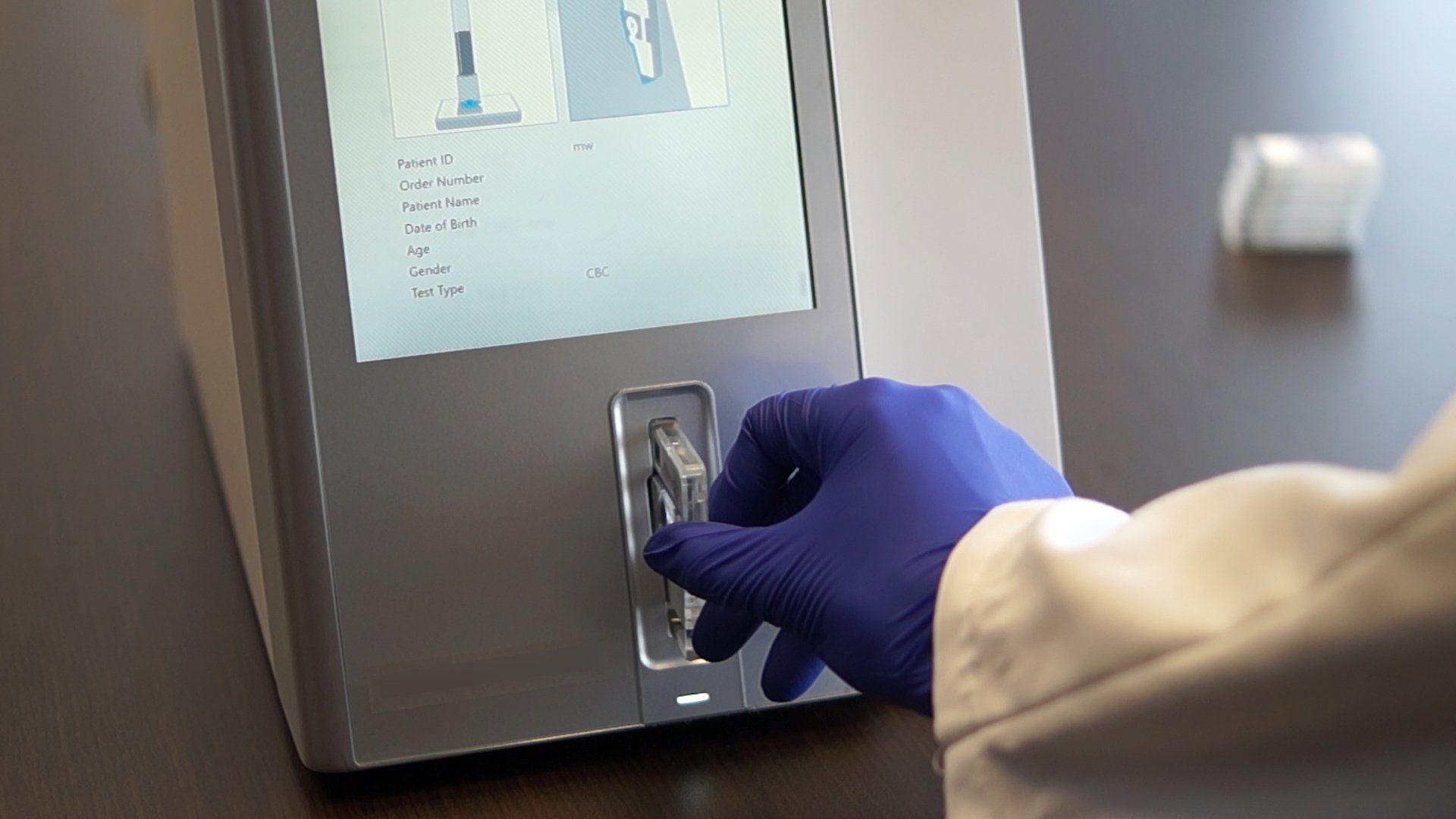
Diagnostic card inserted into a reader
A laser-processed card in its reader.

Materials we process here

Questions we get asked

How do you hold tolerance on laminates that move with humidity?

The machine reads registration features on each sheet and warps the toolpath to the sheet's actual geometry. The part is cut to where the material is, not where the CAD says it should be.

The fastest way to find out is to send us the material.

Trials in the PhotonX lab come back as processed samples and a written report — not a proposal.