

Material family
Glass, Wafers & Wide-Bandgap Substrates
Hard, brittle, and heat-sensitive substrates — glass, silicon, silicon carbide (SiC), gallium nitride (GaN), sapphire, ceramics — micromachined with femtosecond pulses where a saw chips and a nanosecond laser cracks.
Also called: glass-core substrate · borosilicate glass · silicon wafer · silicon carbide · gallium nitride · sapphire · technical ceramics
- Wavelengths
- Femtosecond NIR (1030 nm), green (515 nm), or UV (343 nm), chosen for the substrate's absorption and the feature's edge requirement; UV for polymer layers
- Pulse regime
- Femtosecond, single-pulse and burst-mode; picosecond where throughput outweighs edge quality
- Why the pulse regime matters →
Why these wavelengths
How deep a wavelength penetrates before it is absorbed decides which layer it heats and how much of the pulse reaches the next one. This family’s materials are on the chart. Add others to compare. Every curve is computed from published optical constants, not from our own claims. The sources are in the table below the chart.
Materials on the chart — up to 6 at a time
Gold lines are the laser wavelengths LasX runs; click a laser label to jump to it. Curves stop where the material is transparent for practical purposes — polymers below 1 cm⁻¹ (the datasets’ detection floor), glasses below 0.01 cm⁻¹ (penetration beyond 1 m).
Values at the laser wavelengths, and sources
| Material | 355 nm | 532 nm | 1064 nm | 9.36 µm (9.4 µm laser line) | 10.2 µm | 10.6 µm | Source |
|---|---|---|---|---|---|---|---|
| Fused silica | — | — | — | 27,517 cm⁻¹ 363 nm | 530 cm⁻¹ 19 µm | 253 cm⁻¹ 40 µm | Franta et al. 2016 (fused-silica plate) via refractiveindex.info, CC0 |
| Borosilicate (BK7) | 0.023 cm⁻¹ 43 cm | — | — | 21,343 cm⁻¹ 469 nm | 15,125 cm⁻¹ 661 nm | 7,870 cm⁻¹ 1 µm | SCHOTT N-BK7 catalog (0.3–2.5 µm); Lane 1990 (5–20 µm) via refractiveindex.info, CC0 |
| Soda-lime glass | 0.3 cm⁻¹ 3.4 cm | 0.043 cm⁻¹ 23 cm | 0.6 cm⁻¹ 1.7 cm | 14,517 cm⁻¹ 689 nm | 12,308 cm⁻¹ 813 nm | 8,817 cm⁻¹ 1 µm | Rubin 1985 (clear float; far-IR set) via refractiveindex.info, CC0 |
| Sapphire | — | — | — | 880 cm⁻¹ 11 µm | 1,264 cm⁻¹ 8 µm | 1,500 cm⁻¹ 7 µm | Querry 1985 (α-Al₂O₃, ordinary ray) — shown only above 7.5 µm where its k is resolved via refractiveindex.info, CC0 Transparent 0.17–5.5 µm (Crystran); the curve begins where the dataset resolves absorption. |
| Silicon | 1,044,532 cm⁻¹ 10 nm | 7,684 cm⁻¹ 1 µm | 9.7 cm⁻¹ 1.0 mm | — | — | — | Green 2008 (band-to-band) via refractiveindex.info, CC0 |
— : outside the dataset, or below its detection floor (transparent for practical purposes). Non-metals: α = 4πk/λ; penetration depth 1/α is where 63 % of the beam has been absorbed. Metals: A = 1 − R at normal incidence. All optical constants from the refractiveindex.info database (public domain, CC0); literature points as cited. Full source list and verification notes: docs/charts in the site repository.
Process data
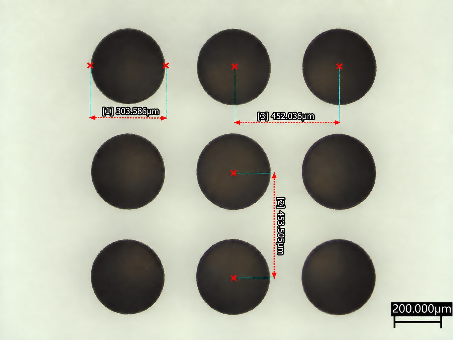
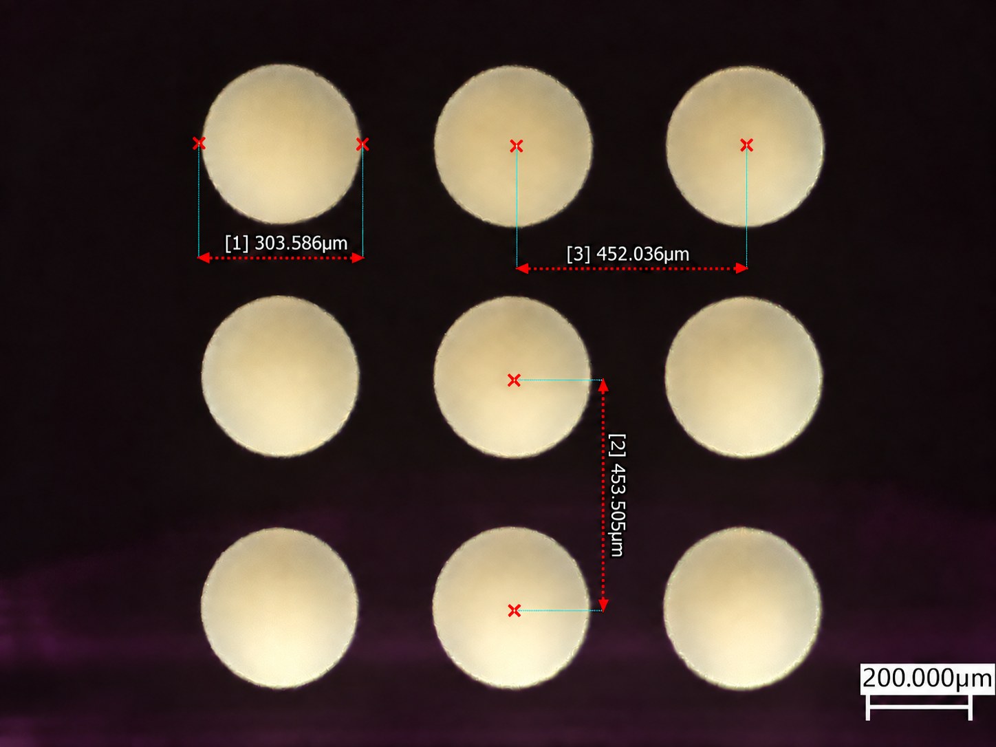
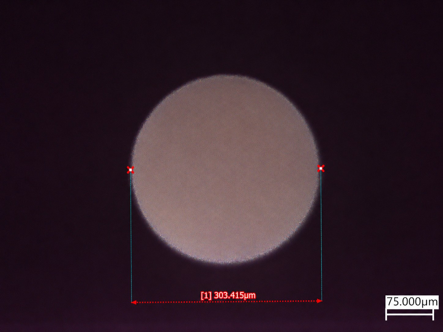
| Via / hole diameter | Trial data requiredSet by wavelength, focus, and burst regime. Measured per substrate and thickness. 300 µm vias on a 450 µm pitch are in development in the PhotonX lab (2026). |
|---|---|
| Heat-affected zone | Trial data requiredThe number that decides yield in glass, SiC, and GaN. |
| Edge chipping and micro-cracking | Trial data required |
| Throughput at specification | Trial data requiredCoupled to feature geometry. Established in the lab before a machine is quoted. |
Entries marked “trial data required” have not been run on your specific construction. We publish only what we have measured.
Typical constructions
- Borosilicate and soda-lime glass, 0.2–2.0 mm, bare and metallized
- Silicon wafers and panels, bare and with low-k dielectric stacks
- Silicon carbide and gallium nitride wafers and dies
- Sapphire and technical ceramics (alumina, aluminum nitride)
- Thin metal films and seed layers on dielectric substrates
- Polyimide and polymer interposers and die-attach films
What usually decides it
Every substrate on this list fails differently under heat. Glass cracks, SiC and GaN delaminate, and low-k stacks peel. That is why the pulse regime matters more than the power. Femtosecond processing, correctly timed on a scanner, keeps energy in the feature and out of the surrounding material. The trial establishes the process window, and the report documents it.
The datasheet number that matters here is not power. It is what the substrate looks like fifty microns from the feature. Three families of work share this page because they share a pulse regime. They do not share a process.
Glass — through-glass vias and glass-core substrates
Advanced packaging is moving from organic to glass-core substrates. The through-glass via is the feature that makes a glass core useful. Femtosecond pulses on a scanner modify or ablate the glass without the micro-cracking that a nanosecond source leaves behind. The same source cuts and singulates panels, and the trial measures edge condition against the downstream finishing requirement. Four numbers decide yield: via diameter, taper, sidewall roughness, and the crack-free zone around each hole. All four are measured on the trial parts.
Current development in the PhotonX lab drills 300 µm vias on a 450 µm pitch in glass. Diameter and pitch hold within a few microns of nominal across the array. Taper is the parameter still being driven down. It is also the first number a packaging engineer asks for, so we report it when the trial parts come back.
Ceramics — marking and serialization
Alumina and aluminum nitride carry the power modules and sensor packages that need a durable, readable identifier. Marking a ceramic is a controlled surface modification. Nothing is cut. The goal is a high-contrast mark that survives sintering, plating, and thermal cycling. The mark must not introduce a crack that propagates later. UV and short-pulse sources give the contrast. The scanner gives the throughput to serialize every part on a panel.
Semiconductor substrates — scribing and singulation
Silicon carbide and gallium nitride power devices are cut from wafers that a saw chips and a thermal laser delaminates. Femtosecond scribing keeps energy in the kerf and out of the active area. The die edge stays intact, and the street can be narrower than a saw allows. The same process scribes silicon with low-k stacks and singulates thin dies from tape. Heat-affected zone and edge chipping are the yield numbers. Throughput is coupled to feature geometry, and we establish it in the lab before we quote a machine.
In production
Fill in the missing numbers with your actual material.
Every trial adds to the measured record behind these pages. It also adds to the process model we are building to predict the window before the first test piece is cut.