Skip to content
LasX — The Laser Experts
Contact us

Industry

Semiconductors & Advanced Packaging

LasX develops scanner-based ultrashort-pulse laser processes for semiconductor back-end and advanced packaging — through-glass vias and glass-core substrate drilling, scribing and singulation of glass, silicon, SiC, and GaN, and selective ablation of thin films on dielectrics — and builds the femtosecond workstations and multi-head machines that run them. We are a laser process and machine-tool company, not a lithography supplier; the work starts where the wafer or panel leaves the fab and needs a hole, a scribe, or a pattern that a saw or a mask cannot make.

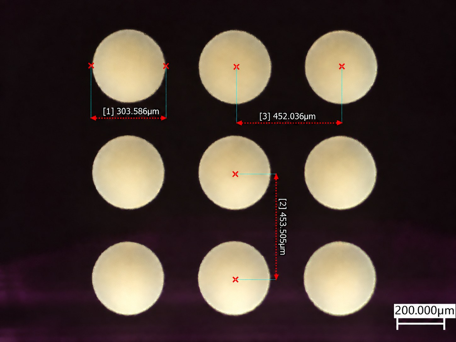
3 × 3 array of 300 µm laser-drilled through-glass vias on a 450 µm pitch, transmitted-light micrograph with measurements
10 nsController output timing resolution
10 MHzIndividual pulse control
NIR · green · UVFemtosecond wavelengths in the lab

Applications

What LasX equipment does in Semiconductors & Advanced Packaging

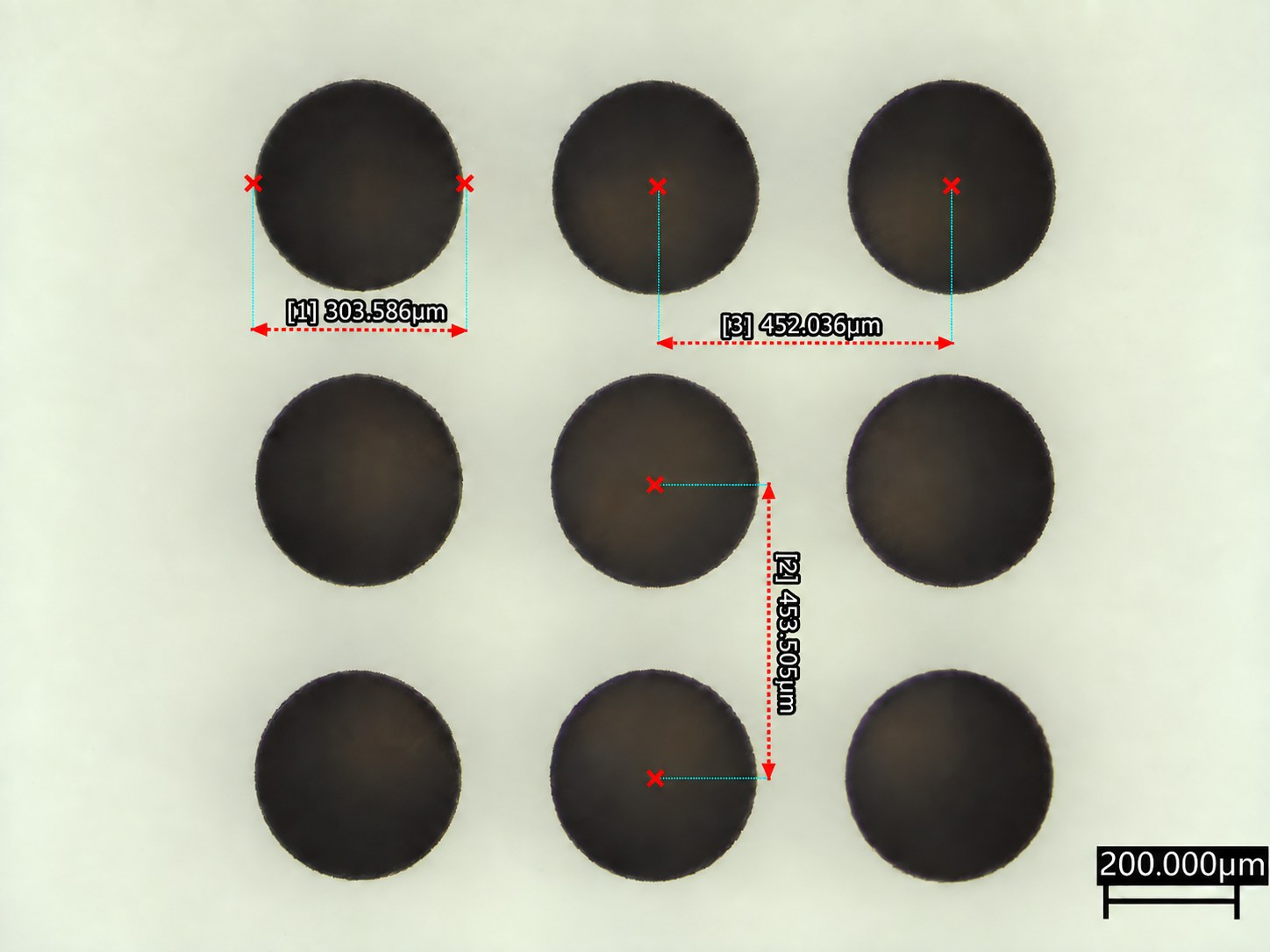
3 × 3 array of 300 µm laser-drilled through-glass vias on a 450 µm pitch, reflected-light micrograph with measurements
Drilling

Through-glass vias and glass-core drilling

300 µm vias on a 450 µm pitch, laser-drilled in glass in the PhotonX lab (2026). Diameter and pitch hold within a few microns of nominal; taper and sidewall condition are the development targets. Feature metrology comes in a written report.

See it on your materialSend a sample →
Cutting

Scribing and singulation

Scribing and singulation of glass, silicon, SiC and GaN. Ultrashort pulses keep the heat-affected zone and micro-cracking down.

Why laser, in this market

01

Advanced packaging needs holes, scribes, and patterns lithography does not make

Chiplets, high-bandwidth memory, and 3D heterogeneous integration are moving substrates to glass and to thicker panels. Through-glass vias, glass-core drilling, and crack-free singulation are laser jobs — scanner-based femtosecond jobs — and they sit alongside lithography, not in place of it.

02

Ultrashort pulses, precisely placed

A femtosecond pulse removes material before heat spreads, which is what keeps the heat-affected zone and micro-cracking down in glass, SiC, and GaN. Proton λ controls pulse output at 10 ns timing resolution, and pulse-on-demand is designed to hold pitch and energy through acceleration and micro-vectors; achieved placement is measured on the substrate in the trial.

03

Developed on your substrate before you buy anything

Wavelength, burst regime, fluence, and scan strategy are chosen on your actual material in the PhotonX lab, with feature metrology and HAZ characterization in a written report. The trial produces the starting recipe and process record for the workstation you buy, or for our floor while your volumes grow.

Buy the equipment

Buy the equipment

ExactPro runs wafer, panel, and substrate work — wafers to 300 mm and 310 mm panel-level packages, with 510 × 515 mm glass interposer and 600 × 600 mm PLP on the 670 mm bed. In its femtosecond configuration that means an NIR, green, or UV ultrashort-pulse source, scanner-based delivery, automated fiducial registration, and Proton λ pulse-on-demand timing. Multi-head and roll-to-roll configurations for volume are engineered as custom equipment.

  • Controller output timing resolution of 10 ns; individual pulse control at up to 10 MHz. Optical pulse placement depends on the source, scanner, and process configuration
  • Registration to fiducials with X/Y/θ and four-point distortion correction
  • XY-stage processing of multi-feature panels, registered sheet by sheet
  • Wavelength and burst regime chosen for the substrate, proven in the lab before the build
Have us make the parts

Have us make the parts

Process development and pilot production in the PhotonX lab and on the LasX floor — feasibility coupons through qualified pilot lots — while your packaging roadmap and volumes settle. Parameters transfer to a machine of your own when they are ready.

  • A written process report — parameters, feature metrology, edge and HAZ characterization
  • Pilot production without capital until volumes justify a machine
  • A recipe that moves with you to a workstation on your floor

The semiconductor industry's laser conversation has moved from "specialized tool" to "fundamental step" in a few years, and the reason is packaging. Once the substrate is glass and the stack is three-dimensional, the features that connect it are made by a beam.

LasX does not make lithography tools and does not intend to. What we make is the scanner-based ultrashort-pulse machine tool that sits next to them — and, before that, the process that proves your substrate on our floor first.

More from production

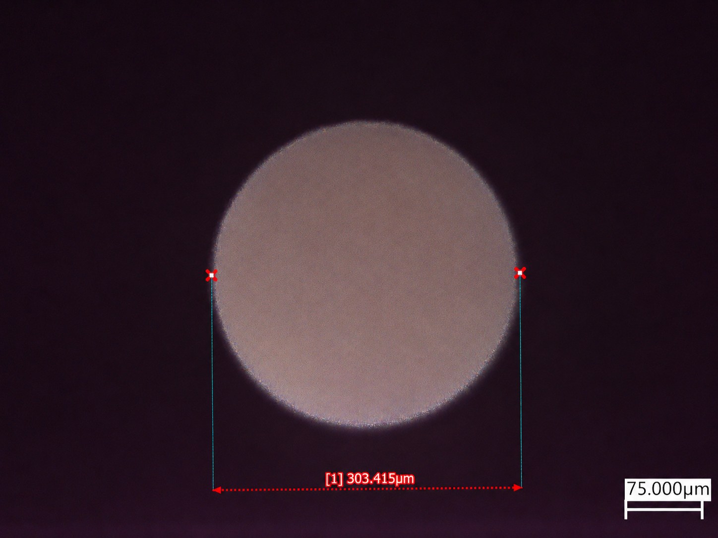
Single laser-drilled through-glass via in transmitted light, measured at 303 µm
One via from the array in transmitted light, measured at 303 µm across. Process development in the PhotonX lab, 2026.
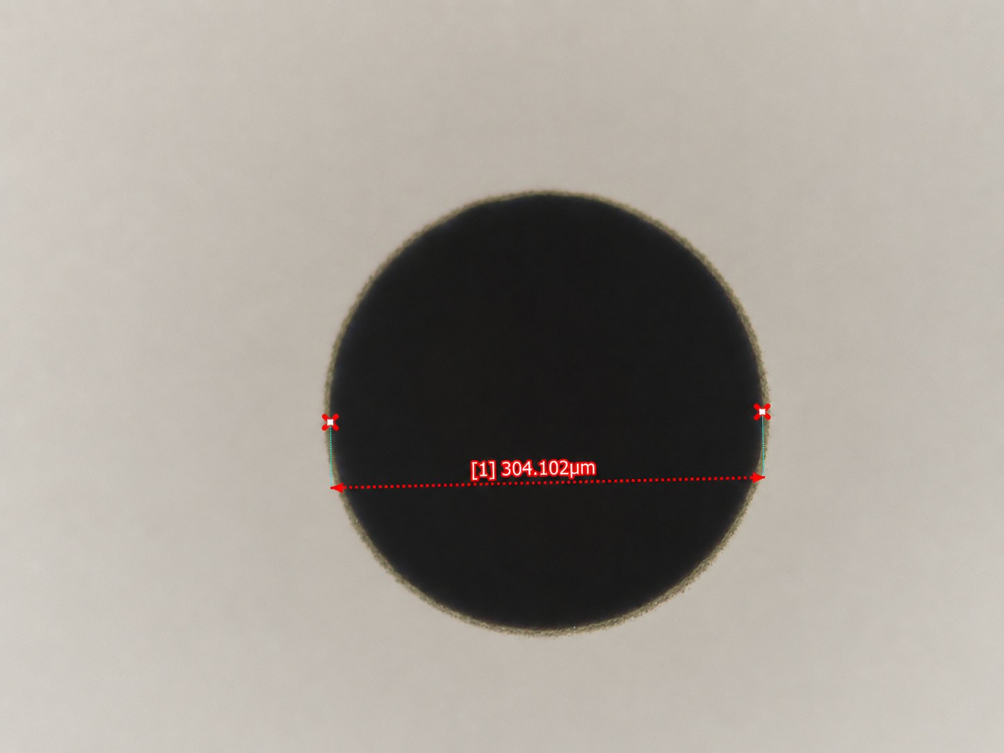
Single laser-drilled through-glass via in reflected light, measured at 304 µm
The same via in reflected light, 304 µm. The light rim outside the aperture is the tapered sidewall seen from above — taper is the parameter still being driven down.

Questions we get asked

Is LasX a lithography or wafer-fab equipment supplier?

No. We build scanner-based laser machine tools and develop the processes that run on them. The work starts after the fab — vias, scribes, singulation, thin-film patterning, and interposer cutting in back-end and advanced packaging — where a focused ultrashort-pulse beam is the right tool.

Which substrates have you processed?

Glass (borosilicate and soda-lime), silicon, silicon carbide, gallium nitride, sapphire, technical ceramics, polyimide and other polymer interposers, and thin metal films on dielectrics. Whether a given construction meets a given specification is answered by a trial, not a datasheet — send the material.

How do you handle through-glass vias at volume?

Scanner-based delivery with pulse-on-demand timing keeps energy per pulse constant through the scan, and vision registration holds the via field to fiducials across the panel. Throughput and via geometry are coupled; a trial on your glass thickness establishes both before a machine is quoted.

The fastest way to find out is to send us the material.

Trials in the PhotonX lab come back as processed samples and a written report — not a proposal.